


NB3RL02FCT2G Datenblatt

NB3RL02FCT2G Datenblatt
Total Pages: 9
Größe: 318,06 KB
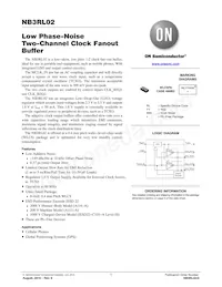
ON Semiconductor
Website: http://www.onsemi.com/
Dieses Datenblatt behandelt 1 Teilenummern:
NB3RL02FCT2G
|
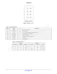
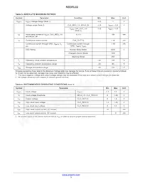
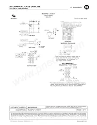
Hersteller ON Semiconductor Serie - Typ Fanout Buffer (Distribution) Anzahl der Schaltkreise 1 Verhältnis - Eingang: Ausgang 1:2 Differential - Eingang: Ausgang No/No Eingabe Clock Ausgabe LVCMOS Frequenz - max 52MHz Spannung - Versorgung 2.3V ~ 5.5V Betriebstemperatur -40°C ~ 85°C Montagetyp Surface Mount Paket / Fall 8-WFBGA, WLCSP Lieferantengerätepaket 8-WLCSP (1.57x.77) |